A joint research team, led by Professor Yung Doug Suh of UNIST, who also serves as Associate Director of the Center for Multidimensional Carbon Materials within the Institute for Basic Science (IBS) and Professor Kyoung-Duck Park from POSTECH, has succeeded in realizing a high-efficiency quantum light source that emits bright lights even at room temperature. The achievement overcomes a longstanding limitation of two-dimensional semiconductors—atomically thin materials typically about 100,000 times thinner than a human hair—which previously required either cryogenic temperatures or complex electrical gating structures to produce efficient light emission.
At the heart of the study are excitons, the light-emitting quasiparticles that form when electrons bind with “holes”—the absence of an electron that behaves like a positive charge—in a semiconductor. In two-dimensional semiconductors, excitons are especially important because they can enable ultrathin and highly efficient optical devices. However, there has been a major problem: at room temperature, excitons tend to spread out too easily, making it difficult to generate bright light from a precise location.
Recently, researchers have become increasingly interested in localized excitons—excitons that are trapped in a confined nanoscale region. A useful analogy is a ball rolling on a flat floor versus a ball sitting in a bowl. On a flat surface, the ball moves around freely, but in a small hollow, it remains trapped in one place. Localized excitons behave similarly: once confined, they can emit light more stably and with better control over wavelength, making them attractive candidates for ideal quantum light sources.
But room temperature makes this difficult. As thermal energy rises, excitons can escape from the trapping region, just as a ball may bounce out of a shallow bowl. At the same time, excess charges remaining in the material can interact with excitons or drain away their energy, causing the system to lose energy as heat instead of light. For this reason, the light-emission efficiency of localized excitons in two-dimensional semiconductors has typically remained below 1% under ambient conditions.
To overcome this challenge, the team designed a 500-nanometer nanohole structure beneath a monolayer of MoS2, a representative two-dimensional semiconductor. This nanohole acts like a nanoscale bowl, naturally funneling excitons toward its center and confining them to a tiny region. According to the researchers’ simulations, about 98% of excitons in the nanohole region were funneled into the center and formed localized exciton states, indicating highly efficient confinement within the nanoscale region.
At the same time, the researchers addressed another major source of loss: excess electrons in the material. During the transfer process used to place the MoS2 layer onto the gold substrate, a thin residual water layer naturally forms at the interface. This layer acts as a dielectric barrier that prevents efficient charge transfer, allowing excess electrons to remain in the semiconductor and degrade emission. By applying thermal annealing, the team removed this water layer and enabled electrons to flow from the MoS₂ into the gold substrate. This effectively neutralized the material and greatly suppressed nonradiative loss pathways.
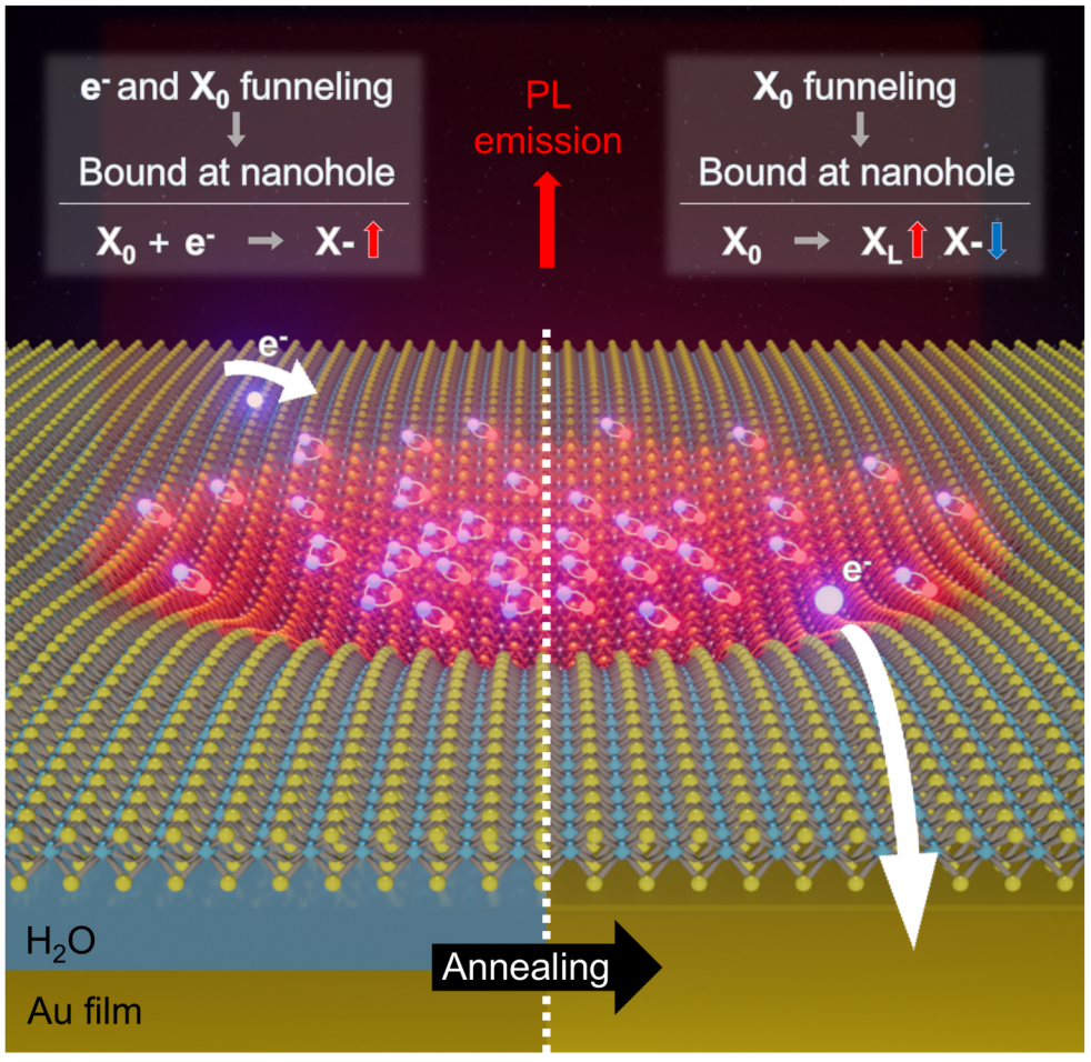
As a result, the system produced bright localized exciton emission under ambient conditions, with the photoluminescence quantum yield increasing by about 130 times compared with the pre-annealed state. The researchers report that the quantum yield in the nanohole region increased from 0.076% (basically unusable) to about 10% (clearly visible bright light), far above the typical value for pristine monolayer MoS₂ at room temperature.
By using the quantum confinement effect to trap light-emitting excitonic states within an extremely small region, the researchers demonstrated a practical route toward bright and stable quantum emission over large areas.
This result is significant because it shows that quantum emitters made from two-dimensional semiconductors can achieve brightness and stability approaching that of quantum dots used in QLED displays, while retaining the additional advantages of atomically thin materials. The work also suggests a path toward even more advanced devices. By making the nanostructures smaller and further optimizing the optical excitation conditions, the researchers believe it may become possible to achieve high-efficiency single-photon emission at room temperature, something that has remained extremely challenging until now.
Professor Kyoung-Duck Park said, “The key achievement of this study is that we realized a quantum light source that emits brightly even at room temperature by gathering and confining light-emitting particles into a single nanoscale point. This structure can serve as a foundation for a wide range of future photonic and quantum devices.” The team also demonstrated that the localized exciton emission could be dynamically and reversibly controlled. By applying gigapascal-scale pressure using the tip of an atomic force microscope, they were able to modulate the strain at the nanohole and thereby tune the behavior of the localized excitons. In annealed samples, this led to an approximately 120% increase in localized exciton emission intensity, and the effect disappeared when the pressure was released, showing that the process is fully reversible.
Associate Director Yung Doug Suh of IBS said, “An important aspect of this work is that we were able to dramatically improve performance by precisely controlling how light is generated and lost in a two-dimensional semiconductor. This technology could become an important turning point toward future room-temperature single-photon sources.”
Another important aspect of the study is its practical scalability. Many previous strategies for realizing efficient localized exciton emission relied on complex electrical device architectures or cryogenic environments, both of which make real-world implementation difficult. In contrast, the present method uses a relatively simple combination of nanostructuring and thermal processing. Because the approach is compatible with established semiconductor wafer-scale fabrication processes, the work opens the door to scalable, integrated quantum light-source technologies for applications, such as quantum communication, quantum computing, and next-generation nano-LEDs.
Beyond quantum communication and quantum computing, the researchers say the platform may also be useful for high-efficiency nanoscale light sources, tunable optoelectronic devices, and future nanophotonic technologies. More broadly, the work provides a new design strategy for controlling excitons in low-dimensional materials: by simultaneously confining excitons spatially and neutralizing unwanted charges, it becomes possible to stabilize bright quantum emission even under ordinary room-temperature conditions. The findings of this research were published in Science Advances on March 13, 2026.
Yung Doug Suh
Professor, Department of Chemistry, UNIST
Associate Director, IBS Center for Multidimensional Carbon Materials (CMCM)
E: ydougsuh@gmail.com
William I. Suh
Public Information Officer IBS Public Relations Team
T: +82-42-878-8137
E:willisuh@ibs.re.kr
Story Source
Materials provided by the Institute of Basic Science.
Notes for Editors
The online version of the original article can be found HERE.
Journal Reference
Taeyoung Moon, Hyeongwoo Lee, Jihae Lee, et al ., “Highly radiative emission of room temperature–localized excitons enabled by charge-neutralized 0D quantum wells in 2D semiconductors,” Sci. Adv., (2026). DOI: 10.1126/sciadv.ady2186